> For the complete documentation index, see [llms.txt](https://docs.voltera.io/docs/llms.txt). Markdown versions of documentation pages are available by appending `.md` to page URLs; this page is available as [Markdown](https://docs.voltera.io/docs/v-one/learn-v-one/v-one-projects/punk-console-project/4.-printing-the-circuit.md).
# 4. Printing the Circuit
### Punk Console: Printing
The key reason we are printing right after drilling (without removing the substrate) is because we will have a perfect alignment between the ink and drill hole. We can confidently probe and print our first layer without having to worry about our alignment for the top layer.
### Printing the top layer
Jump into the print workflow and click **ALIGNED**. Then load the following files:
* [Punk\_Console.GTL](https://assets.ctfassets.net/e6vf9wdhbae5/5b9HF0ozHbIBJYOcJ20tml/e7e3490ee81866d248206f483f5e64ba/Punk_Console.GTL)
* [Punk\_Console.TXT](https://assets.ctfassets.net/e6vf9wdhbae5/7d4gVT7yuj14JSeObt6gLU/01c3a3893c294089a44310a547b1bdf3/Punk_Console.TXT)
The top layer of the circuit looks like this:
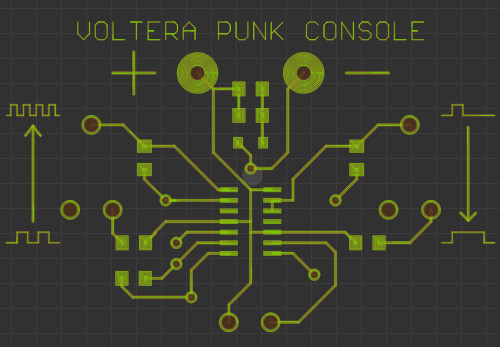
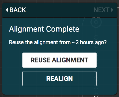
When it comes time to position the print, click the 'Reuse Alignment' button. The alignment that was used during the drilling step will be loaded.
Continue with the print workflow, it will be very similar to printing a single sided board except the **calibration pattern may print on top of holes**. This is normal and does not have negative side effects. You may wipe down the ink afterwards.
{% hint style="info" %}
The calibration pattern may print on top of drilled holes. This is normal and will not have any negative side effects!
{% endhint %}
### Baking your board
To bake your board remove the **sacrificial layer** to ensure the board reaches the curing temperatures.
{% hint style="warning" %}
Remove the sacrificial layer before you start the bake to ensure the board gets hot enough and the ink cures properly!
{% endhint %}
Then you can place the board back on the heated bed face up to start curing. Conductor 3 no longer requires you to flip your board for this process.
{% hint style="info" %}
The substrates provided with the V-One Drill are made of FR1. You might see the substrate brown a bit after the baking cycle.
{% endhint %}
### Printing the bottom layer
To print the bottom layer, flip the board and clamp it with the blank side up. It is not necessary to mount the sacrificial layer. Start the print workflow and once again choose **ALIGNED**.
Load the following files:
* [Punk\_Console.GBL](https://assets.ctfassets.net/e6vf9wdhbae5/1BzdFetYFZNdohRRI87LGo/b00b12d27d0bc328cf111e6bf0ce5967/Punk_Console.GBL)
* [Punk\_Console.TXT](https://assets.ctfassets.net/e6vf9wdhbae5/7d4gVT7yuj14JSeObt6gLU/01c3a3893c294089a44310a547b1bdf3/Punk_Console.TXT)
The drilled holes are used to align the board. The software will automatically pick two holes for you to use, but for this circuit you should override the selection and use the following holes.
#### First Alignment
In the '**Align Circuit**' step, click the following hole and align to it:
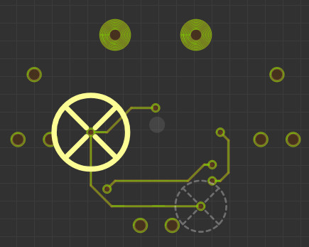
1. Click the **MOVE TO PAD** button to start the pad location process.
2. Use the **arrow keys** to move the printer to the *approximate* location of the pad that is highlighted in the print preview. You do not need to align it perfectly just yet.
3. Click **LOWER** to drop the probe to the surface of the board.
4. Use the **arrow keys** to once again adjust the position of the probe. This time, position the probe in the **center** of the highlighted pad
5. Click **MEASURE** to confirm the pad location.
When you click measure, the probe will record the position and descend into the hole, this is normal.
#### Second Alignment
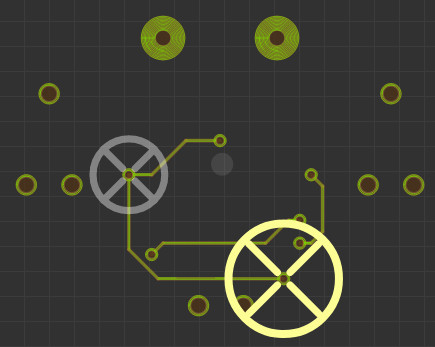
Select the following hole for the second feature and align the probe tip to it:
#### Validate Pads
Before we get to printing the solder paste, use this step to make sure that the pad alignment is accurate.
Click on any pads in the print preview, and the printer will go to the center of the pad. If you notice that the position is off, press the **BACK** button and repeat the Locate Pad steps.
#### Probing, Printing and Baking
Continue through the print workflow following the same steps as when printing the top layer.
After the baking the backside of the board we can add rivets to all of our drilled holes. When you are ready, let's start adding rivets!
---
# Agent Instructions
This documentation is published with GitBook. GitBook is the documentation platform designed so that both humans and AI agents can read, navigate, and reason over technical content effectively. Learn more at gitbook.com.
## Querying This Documentation
If you need additional information that is not directly available in this page, you can query the documentation by asking a question.
Perform an HTTP GET request on the following URL with the `ask` and `goal` query parameters:
```
GET https://docs.voltera.io/docs/v-one/learn-v-one/v-one-projects/punk-console-project/4.-printing-the-circuit.md?ask=&goal=
```
`ask` is the immediate question: it should be specific, self-contained, and written in natural language.
`goal` is what the user is ultimately trying to achieve, the reason they need the answer. Sharing it helps GitBook give you a better, more relevant answer. A goal is most helpful when it describes the outcome the user wants rather than restating the question. For example, with `ask=how do I create an API token`, a goal like `automate deployments from our CI pipeline` lets GitBook tailor the answer to that use case.
The response will contain a direct answer to the question and relevant excerpts and sources from the documentation.
Use this mechanism when the answer is not explicitly present in the current page, you need clarification or additional context, or you want to retrieve related documentation sections.

